The post How to interface Stepper Motor with PIC18F4550 Microcontroller appeared first on PIC Microcontroller.
How to interface Stepper Motor with PIC18F4550 Microcontroller
How to display text on 16×2 LCD using PIC18F4550
Several automated and semi-automated devices require a message to be displayed in order to indicate their working status. In continuation to LCD interfacing with PIC18F4550, this article explains how to display a message or string on a 16×2 character LCD.
In the previous article, a single character was displayed on LCD by properly configuring its data and command registers. A string is nothing but a sequential arrangement of several characters that can be displayed on LCD by using the programming steps mentioned here. The circuit connections and user-defined functions are same as earlier. The LCD data pins are connected to PortB of PIC18F4550 while the control pins are connected to first three pins of PortA.
· Use lcddata() function to send individual character values of the string to be displayed on LCD.
For more detail: How to display text on 16×2 LCD using PIC18F4550
The post How to display text on 16×2 LCD using PIC18F4550 appeared first on PIC Microcontroller.
How to interface GSM Module with PIC18F4550 Microcontroller
The post How to interface GSM Module with PIC18F4550 Microcontroller appeared first on PIC Microcontroller.
Spectrum analyzer based PIC18F4550
The project demonstrates the implementation of the sound spectrum analyzer for 8-bit microcontroller PIC18F4550 manufactured by Microchip . Spectrum analysis is performed using an optimized fast Fourier transform algorithm (Fast Fourier Transformation, FFT), written entirely in C language. Data Visualization (spectrum) is carried out in real time on a graphical LCD display with a resolution of 128 × 64 pixels.
Key Features:
- sampling rate 20 kHz;
- frequency range 312 Hz – 10 kHz;
- the display speed of 10 frames per second;
- display resolution of 128 × 64 pixels;
To calculate the values of the fast Fourier transform algorithm in the range of sound frequencies necessary to prepare the signal for further processing microcontroller. PIC18F4550 has an integrated multi-channel ADC, which can be used to measure voltage in the range 0 V – 5 V with 10-bit resolution (0-1023).
The main characteristics of the microcontroller:
- core PIC18, the operating frequency to 48 MHz;
- 32 KB Flash-memory programs;
- 2 MByte RAM;
- one 8-bit timer, three 16-bit timers;
- USB interface, SPI interface;
- 13-channel 10-bit ADC;
- 35 I / O lines for general use.
Audio signal from audio line-out is an alternating signal wave with an amplitude of about 1 V. The lower oscillogram clearly shows the sinusoidal tone frequency of 5 kHz (reference point on the chart W2 ).
If such a file directly to Segal ADC of the microcontroller, we get only a small range of input voltage (0 V – 0.5 V), ie we obtain the values of only the top of the wave and the calculation of FFT algorithm will be incorrect.
In order to get the correct calculations, we need over the original signal to do some action. First you need to amplify the signal in order to use the entire working range of the ADC of the microcontroller (0 V – 5 V). In the second stage, we need to shift the signal at 2.5 V (“virtual” 0) to the ADC can capture all the values of the analog signal. Thus, the microcontroller will be able to do sampling positive and negative half-wave signal.
To this end, the device used a simple on-chip amplifier LM386-1 – we solve the first condition – the signal gain. Nutrition amplifier is +5 V, and because of this, we perform the second condition – positive offset signal. With the same purpose is permissible to use rail-to-rail operational amplifier (op amp output signal c scale, equal to the voltage supply).
Oscillogram below shows the shape of the signal after the amplifier LM386-1 (control point on the chart W3 ).
The device has a stereo input J4, but with two resistors (R1, R2) par 10k done mixing the two signals. With the potentiometer R3 is possible to regulate the amplitude of the signal. The output signal from the amplifier passes through a simple RC filter is 10 kHz, and the resulting signal to the input of the ADC of the microcontroller.
RC filter 10 kHz in our case used as a filter of “smoothing” for the FFT, which can not correctly detect a signal with a frequency above 10 kHz. It is worth noting: RC filter – the filter is simple and very inefficient, but this type of filter was chosen because of ease of implementation, since required all two passive elements. Users can replace this part of the scheme, such as a filter using the operational amplifier.
To display the data using a graphical LCD display ATM12864D , one based on the controller and KS0108B KS0107B. The display connects directly to a microcontroller with 8-bit bus. In addition there are three LEDs, which are used in the test mode conversion, “music-light.” Two buttons SW1 and SW2 are used to switch display modes. The second connector J5 is designed to implement the through channel (eg, headphones). J2 connector is designed to connect the programmer and in-circuit programming of the microcontroller. To supply schemes applied voltage regulator LM7805 .
The developed one-sided printed circuit board is designed for use and installation of components with pin terminals.
However, a schematic diagram of the device is not complicated and can collect it on the breadboard. Possible to use another microcontroller, software compatible with the PIC18F4550 (for example, PIC18F2550 ).
Schematic diagram and printed circuit board (format and expressSCH expressPCB) – download
In the second part of this article, we look at the highlights in the software of the microcontroller.
In the first part Spectrum analyzer based PIC18F4550. Part 1, we met with the scheme, with the appointment of individual nodes and elements, over the principles of operation.
Microcontroller software is written entirely in C language, and it can be conditionally divided into 4 parts.
1. ADC sample data (sampling)
Implementation of sampling analog-digital converter is the channel every 50 ms RA0. This gives us a sampling frequency of 20 kHz (20,000 times per second). For the Fourier transform is very important that the samples were uniform and accurate. With this purpose in the subroutine get data from ADC introduced a short time delay, which was calibrated using an oscilloscope connected to the control point W4 on the board. Square-wave period as measured in this reference point should be exactly 50 microseconds. ADC works with a full 10-bit resolution, and the results are shifted down to 512 to implement a “virtual earth” input signal. This means that the resulting data will be in the range from -512 to 512, as required for the mathematical transformation FFT.
The procedure for obtaining the samples will take a little time to 32 ms (64 × 50 microseconds) for each cycle.
2. 16-bit FFT
Subroutine, which implements the calculation algorithm FFT, was found on the Web so (link to the original code is in the source code at the end of the article). Math FFT is complex and difficult to understand. The code has been slightly simplified and adapted for the PIC18F4550. Since the microcontroller has a hardware multiplier 8 × 8 as part of its arithmetic and logic devices have been optimized computing, allowing the compiler to correctly use the features of the microcontroller.
For more detail: Spectrum analyzer based PIC18F4550
The post Spectrum analyzer based PIC18F4550 appeared first on PIC Microcontroller.
Minty JDM PIC Programmer using PIC18F4550 microcontroller
Minty JDM PIC Programmer
This project details how to build a JDM style programmer to program PIC Microcontrollers using Microchip’s ICSP (In Circuit Serial Programming) and freeware software (PICPgm). Total project cost: less than $10. This device has been tested on both the PIC16F877 and PIC18F4550. Check the PICPgm website to see compatibility with other PIC microcontrollers.
I used information from http://www.olimex.com/dev/images/PIC/PIC-USB-4550-sch.gif and Ian’s excellent instructible http://www.instructables.com/id/Business-Card-PIC-Programmer/ to complete this project.
Step 1
Parts and Tools
Most of these parts are fairly common and can be found at Digikey, All Electonics, or Radio Shack:
(1) DB9 Female Serial port connector w/ at least a 5 wire cable attached (Connector was $4.50)
(1) Cable with 5 wires and a connector to connect to PIC circuit (I used an old mouse cable)
(1) 1.5K Ohm Resistor ($0.14 ea)
(1) 10K Ohm Resistor ($0.14 ea)
(4) 1N4148 Diodes ($0.18 ea)
(1) 8.2V Zener Diode ($0.32 ea)
(1) 5.1V Zener Diode ($0.27ea)
(2) BC547 Transistors ($0.41 ea)
(1) 22uF Tantalum Capacitor ($0.32 ea)
(1) 100uF Electrolytic Capacitor ($0.27 ea)
(1) Small Prototype Board ($1.99 ea)
(1) Small Mint Tin (Had one laying around)
Some small guage wire for connections
Tools required:
– Soldering Iron and Solder
– Wire Strippers
– Multimeter (for checking connections)
Step 2
Layout
I chose to layout my components in a straight line and make the connections on the back side of the board. Take a look at the schematic on the next step if you wish to have a different layout. If you use this layout, MAKE SURE YOU GET THE DIODES, CAPS, AND TRANSISTORS PLACED PROPERLY! Notice that the last diode is placed opposite of the others. Make sure you have the capacitors oriented to connect the negative lead to ICSP pin #3.
Step 3
Schematic
Here is the schematic for circuit. The circuit uses power from the serial port to power the PIC microcontroller during programming. Some USB to Serial converters do not work with this circuit because of the voltage needed on the PIC’s mclr pin. This circuit works best with on board ports or serial cards. For the ICSP pins, they are connected to the microcontroller as follows:
1. MCLR Pin
2. VDD Pin(s)
3. VSS Pin(s)
4. PGC Clock Pin
5. PGD Data Pin
Step 4
Soldering
Once the components are in place, solder the pins together as directed by the schematic in the previous step. Use wire to jumper points together as needed. I tested all connections a couple times with the multimeter to make sure that everything was connected properly and that points weren’t shorted together. I’ve attached a schematic to this step that is a mirrored version of the original, it comes in handy when soldering and testing the connections. It shows the view of the circuit as seen from the solder side.
For more detail: Minty JDM PIC Programmer using PIC18F4550 microcontroller
The post Minty JDM PIC Programmer using PIC18F4550 microcontroller appeared first on PIC Microcontroller.
Seven Segment Multiplexing using PIC18F4550 Microcontroller
As explained earlier, a seven segment interfaced with PIC uses almost an entire port (minimum 7 pins) to display a value. But a real time application, like watch, calculator etc., usually requires at least 3-4 seven segments. In such a case it is not advisable to use a port of the controller for each seven segment. In these cases, multiplexing technique is used to work with more than one seven segment. Here multiplexing of four seven-segments has been explained with PIC18F4550 to display four-digit count from 0000 to 9999.
The data pins (a-g) of all the seven-segments are connected to a single port (Port D*) as shown in the circuit diagram. Transistors BC547 are connected to COM pins of seven-segment for switching. The switching of COM pins is controlled by four pins of PortA.
The post Seven Segment Multiplexing using PIC18F4550 Microcontroller appeared first on PIC Microcontroller.
Audio spectrum analyzer using PIC18F4550
Introduction
This project implements a real-time audio spectrum analyser using a PIC18F4550 8-bit microcontroller. The spectrum frequency analysis is performed by a highly optimised 16-bit Fast Fourier Transformation (FFT) routine coded entirely in C. The output from the FFT is displayed using a 128×64 graphical LCD to allow a real-time view of an audio signal.
Hardware
In order to perform a FFT calculation on an audio signal it is necessary to prepare the audio so the PIC18F4550 can sample the signal. The PIC18F4550 provides several analogue to digital converters (ADCs) which can be used to measure a voltage from 0V to 5V with 10-bit accuracy (0-1023). A typical audio line-out signal is an analogue wave with a peak-to-peak intensity of 2V centred around 0V (i.e. it is an AC signal ranging from +1 to -1V) as shown by the following oscilloscope trace (from pin W2 of the demo board):
The picture shows a full-volume 5000Hz sine wave generated by a PC. If we were to feed this signal directly to the PIC we would only have a very small range of input voltage (0-0.5V) and also we would only be able to sample the top-half of the signal which would make the FFT incorrect.
In order to correctly sample the signal we have to do two things. Firstly we need to amplify the signal to ensure we can use as much of the 0-5V range as possible. Secondly we have to move the signal’s ground (of 0 volts) to a ‘virtual ground’ of 2.5Vs. This will allow the PIC to sample both the positive and the negative sides of the input signal. To do this the demonstration board uses a simple amplifier IC (the LM386-1). Since the IC is powered from a 0V and 5V power supply it has the handy side-effect of also moving the signal into the middle of our required power range. The LM386-1 was used because it is cheap and simple, however you could use a rail-to-rail opamp to achieve the same thing with a few more external components.
The following oscilloscope trace shows the output signal from the LM386-1 (for the signal shown above), the scope voltage range is set to 5 volts (from pin W3 of the demo board):
The hardware mixes the stereo line-in using two 10K resistors which act as a simple mixer. The signal is then passed to the LM386-1 via a 10K potentiometer which allows the signal strength to be adjusted. Next the LM386-1 amplifier output is passed through a simple RC Filter which rolls off the signal at about 10Khz. The resulting signal is then fed into an ADC pin on the PIC18F4550. The 10Khz filter acts as an ‘anti-aliasing’ filter for the FFT which cannot correctly detect signals with a frequency of greater than 10KHz. An RC filter is a very simple type of filter (and very ineffective) but it was chosen since it is easy to build and only requires 2 passive components. Typically a professional spectrum analyser would implement the anti-alias filter at 80% of the Nyquist frequency for the FFT (see below), but since we are so speed-limited with the PIC this is not possible to do in the design.
The demo board also controls a standard 128×64 dot-matrix LCD as well as 3 LEDs (for testing sound-to-light conversion). In addition there are 2 switches to allow the user to control the LCD’s output depending on what is being measured and how it is to be displayed. The second phono socket allows you to pass-through the input signal to another audio device such as headphones or speakers.
For more detail: Audio spectrum analyzer using PIC18F4550
The post Audio spectrum analyzer using PIC18F4550 appeared first on PIC Microcontroller.
How to Implement SPI Using PIC18F4550
The Serial Peripheral Interface (SPI) is a high speed, synchronous, serial communication standard. This communication protocol is basically a Master – Slave implementation where the master device controls the clock based on which the slave devices operate. The master communicates with a slave or a number of slaves in a system through the SPI bus.
The SPI bus requires a minimum of three wires including SDO (Serial Data Out), SDI (Serial Data Input) and SCK (Serial Clock). Since it is a master controller system the SDO is also called MOSI (Master Output Slave Input) and the SDI is also called MISO (Master Input Slave Output).
The SPI is a full-duplex high speed communication protocol. The master and slave can transmit and receive data at the same time. The master is the device which generates clock for all these data transmissions.
Read PIC microcontroller tutorial based on PIC18F4550 microcontrollers in which one of the microcontroller acts as a slave transmitter and the other acts as master receiver.
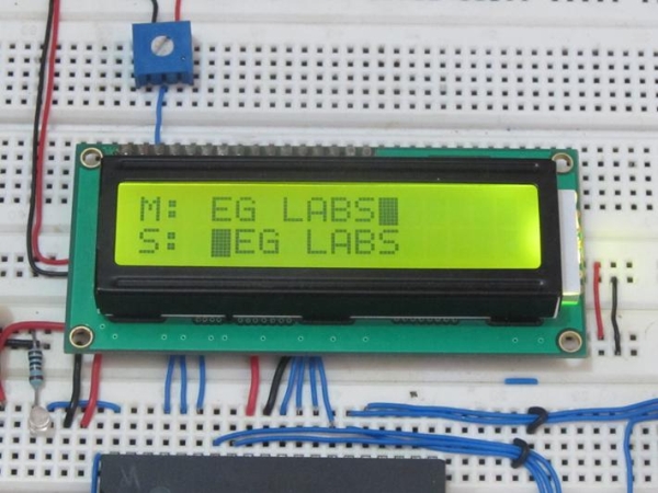
With the help of an LCD, this particular project demonstrates the complete data transfer between a master and slave when both the master and slave are transmitting and receiving the data at the same time.
In PIC18F4550 microcontroller the hardware implementation for the SPI interface can be viewed as a simple SISO (Serial-In-Serial-Out) Shift register controlled by a Clock.
The above diagram is a single buffer implementation of the SPI hardware. The data is shifted into the buffer from the slave device through the SDI (MISO) and the data is shifted out of the buffer to the slave through the SDO (MOSI). The only difference in the hardware configuration of a master and slave device is the direction of the clock. For a master device the clock is always output and for a slave device the clock is always input.
The Clock unit can generate the clock required for the data transmission. In case of a master device the clock is generated by the device and all other devices in the SPI bus send or receive data to the master based on this clock. When the microcontroller is configured as a slave it can only accept the clock from a master device.
On each clock generated or received one bit in the SISO register is shifted from the SDI to SDO. After the eighth clock since the communication starts, one byte of data has been shifted out through the SDO and one byte of data has been shifted in through the SDI. Now the SISO has an entire byte received from the slave while transmitting a byte to the slave.
In PIC18F4550 the Serial Communication registers are not dedicated for the SPI only, but it can be configured for IIC communication also. The entire module is called Master Synchronous Serial Port (MSSP) module. There are a few registers available in the PIC18F4550 which helps to configure the MSSP as an SPI master or slave module. The major registers associated with the SPI communication in the PIC18F4550 are SSPBUF, SSPSTAT and SSPCON1 register.
SSPBUF
The Synchronous Serial Port Buffer (SSPBUF) register is the register which holds the SPI data which needed to be shifted out to the slave or which has been shifted in from the slave. In case of a slave device this register holds the SPI data which needed to be shifted out to the master or which has been shifted in from the master.
SSPSTAT
The Synchronous Serial Port Status (SSPSTAT) register is the register which holds the status of the SPI module. The first two bits and the last bit of this register are only dedicated for the SPI communication.
The SMP bit decides when the master should sample the data, the CKE decides when to transmit data based on the clock transition and the value of BF indicates whether the SSPBUF is full or not (reception complete or not).
SSPCON1
The Synchronous Serial Port Control 1(SSPCON1) register is the register which is dedicated register for the control of SPI only. All the bits of these register are significant and should be carefully set them.
WCOL bit indicates whether a Write collision has been occurred or not, the SSPOV indicates whether an overflow occurred in SSPBUF or not, SSPEN is the bit which is used to enable or disable the SPI module. The CKP bit is used to decide which are the idle state and the active state of the clock. The bits SSPM3 to SSPM0 is used to set the device as a master or slave with required clock frequency for master and SS enabled or disabled for the slave.
The registers are explained with more details in PIC microcontroller
READ AND WRITE OPERATIONS
Whenever the master or slave needs to transmit data, it can simply write the data to the SSPBUF. When the master writes the data to the SSPBUF the clock will get generated automatically and with each clock the data from the SSPBUF is shifted out through the SDO pin bit by bit. When the slave writes into the SSPBUF the data remains there until the master generates a clock which will shift the data out from the slave’s SSPBUF through its SDO pin.
Apart from simply writing into the SSPBUF for data transmission, the master or slave can also read the received data from the SSPBUF. The master and slave should write or read from the SSPBUF in a particular manner only. Read PIC microcontroller tutorial to know more.
TIPS FOR CODING:
The SPI protocol is implemented in different devices in different manner and hence when it comes to the coding one should carefully study all the hardware details regarding the SPI implementation in the device for which the coding should be done. Care should be taken especially on the clock frequency, SPI pin’s multiplexed arrangement, clock polarity settings, use of SS pin and code performance etc. To have clear understanding of code writing visit PIC Microcontroller tutorial.
CODE DETAILS
The code includes a few functions for initializing the SPI module, sending and receiving the SPI data etc. The details of the functions are given below;
Voidspi master_init ( void )
This function is used to initialize the SPI module as a master with the required clock frequency. It also set the clock polarity and when to sample input data and to transmit output data regarding the clock transition states. It also sets the SPI pins as input or output as required by the master. It can also disable all other modules multiplexed into the SPI pins.
Voidspi slave_init ( void )
This function is used to initialize the SPI module as a slave with SS pin enabled. It also set the clock polarity and when to sample input data and to transmit output data regarding the clock transition states. It also sets the SPI pins as input or output as required by the slave. It can also disable all other modules multiplexed into the SPI pins.
unsigned char spi data ( unsigned char tx_data )
This function can send a data byte which it takes as the argument and return the received data byte. The master first write the data and then wait for the data to complete transmission and then read the received data while the slave first wait till all the data bits has been received, and then reads the data followed by a data write.
The functions are explained with more details in PIC microcontroller tutorial.
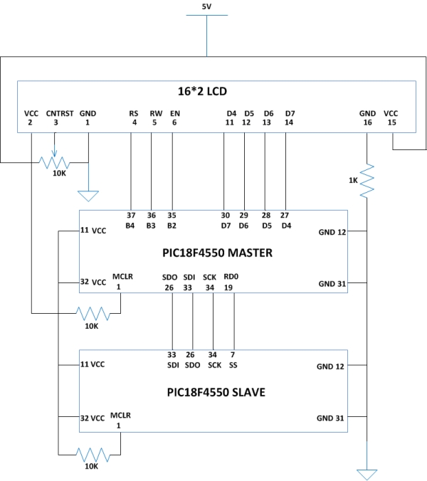
MASTER AND SLAVE AS TRANSMITTER AND RECEIVER
The arrangement below shows how the master transmits some meaningful data to the slave which the slave can receive. The data which the master transmits is displayed in the first line of the 16×2 LCD. The slave then transmits the same data which it has received back to the master which is then displayed in the second line of LCD. In this way the master is doing transmission and reception and the slave is also performing transmission and reception. Since the PIC18F4550 is used as master and slave the capabilities of the SPI module of the PIC18F4550 is exploited to the maximum in this project. The following figure can make the arrangement details more clear;
The post How to Implement SPI Using PIC18F4550 appeared first on PIC Microcontroller.
How to interface RFID with PIC18F4550 Microcontroller

Pin No.
|
Name
|
Description
|
1
|
Vcc
|
Supply Voltage; 5V
|
2
|
GND
|
Ground (0V)
|
3
|
BEEP
|
Beep or LED drive
|
4
|
ANT
|
No Use
|
5
|
ANT
|
No Use
|
6
|
SEL
|
High is RS232, Low is Weigand
|
7
|
RS232
|
TTL output data
|
8
|
D1
|
Weigand Data 1
|
9
|
D0
|
Weigand Data 0
|
The post How to interface RFID with PIC18F4550 Microcontroller appeared first on PIC Microcontroller.
How to work with inbuilt ADC Module of PIC18F4550
A microcontroller, a digital device, can read, execute and transmit only digital signals. On the contrary, the outputs of the most of the transducers are analog in nature. Thus it is hard to interface these transducers directly with controllers. Analog-to-digital convertor (ADC) ICs are one way to make the analog input compatible with the microcontroller. …
How to work with inbuilt ADC Module of PIC18F4550 Continue Reading
The post How to work with inbuilt ADC Module of PIC18F4550 appeared first on PIC Microcontroller.